[Download 41+] Antenna Effect In Vlsi Ppt
View Images Library Photos and Pictures. Full-Custom Design …. TYWu. Outline Introduction Transistor Process Steps Layout Schematic R/C Design Rules Tools. - ppt download PPT - EECE 476: Computer Architecture Slide Set #2: Fundamentals of Computer Design PowerPoint Presentation - ID:3733023 Channel Length Modulation in MOSFET (VLSI Design) – Buzztech Silicon junctionless field effect transistors as room temperature terahertz detectors: Journal of Applied Physics: Vol 118, No 10

. Vlsi OSA | Array of plasmonic Vivaldi antennas coupled to silicon waveguides for wireless networks through on-chip optical technology - WiNOT PPT - EECE 476: Computer Architecture Slide Set #2: Fundamentals of Computer Design PowerPoint Presentation - ID:3733023

CMOS Processing Technology.ppt | Photolithography | Microscope

 Vlsi
Vlsi
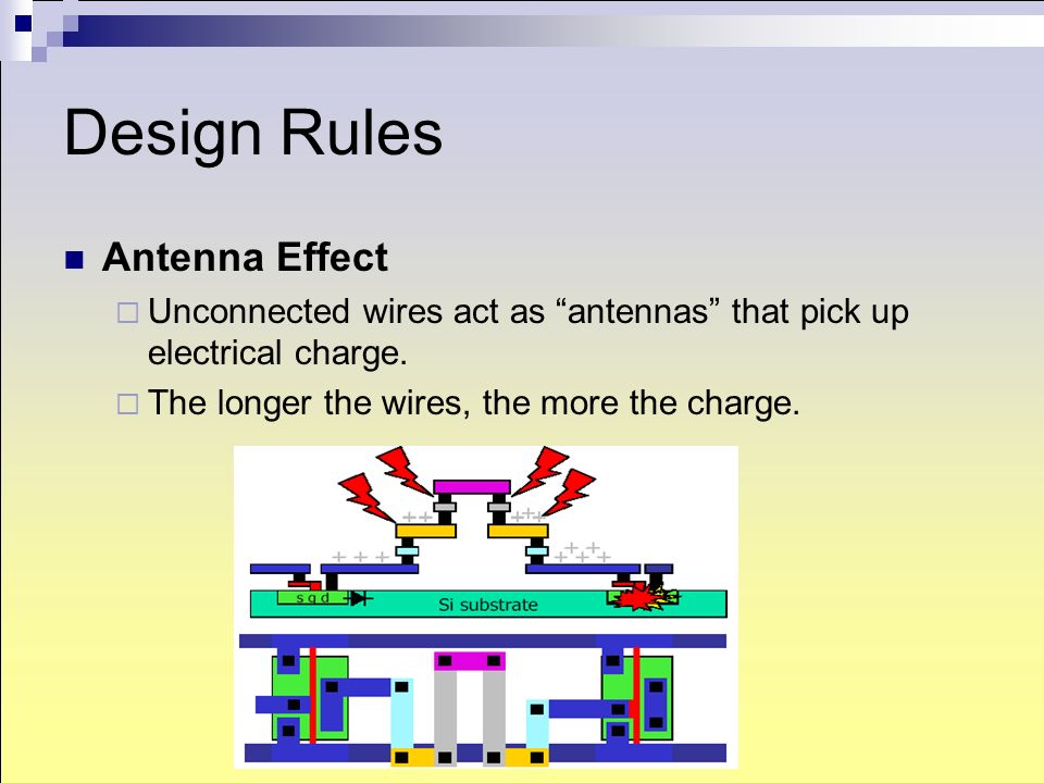
 Antenna effect - Wikipedia
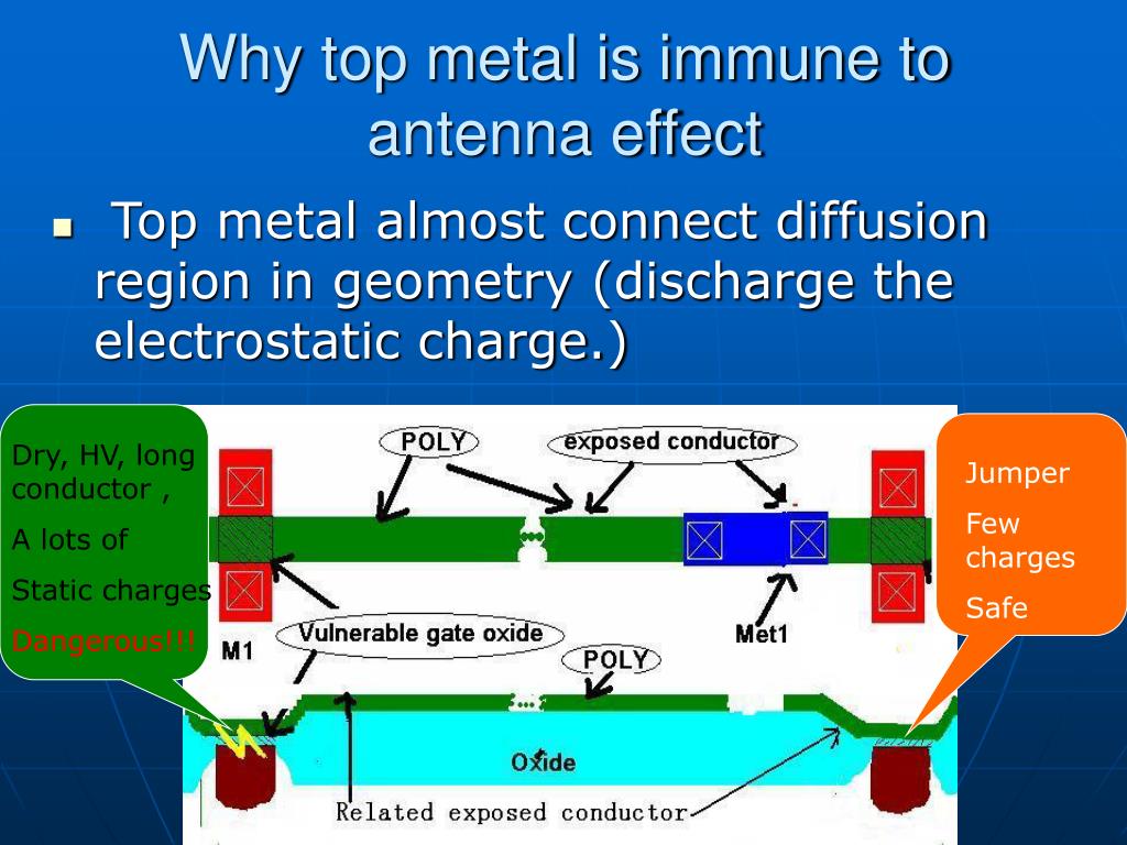 PPT - The common questions in analog layout PowerPoint Presentation, free download - ID:5517738
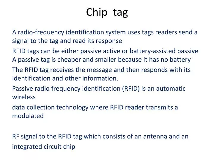 PPT - Chip tag PowerPoint Presentation, free download - ID:6082536
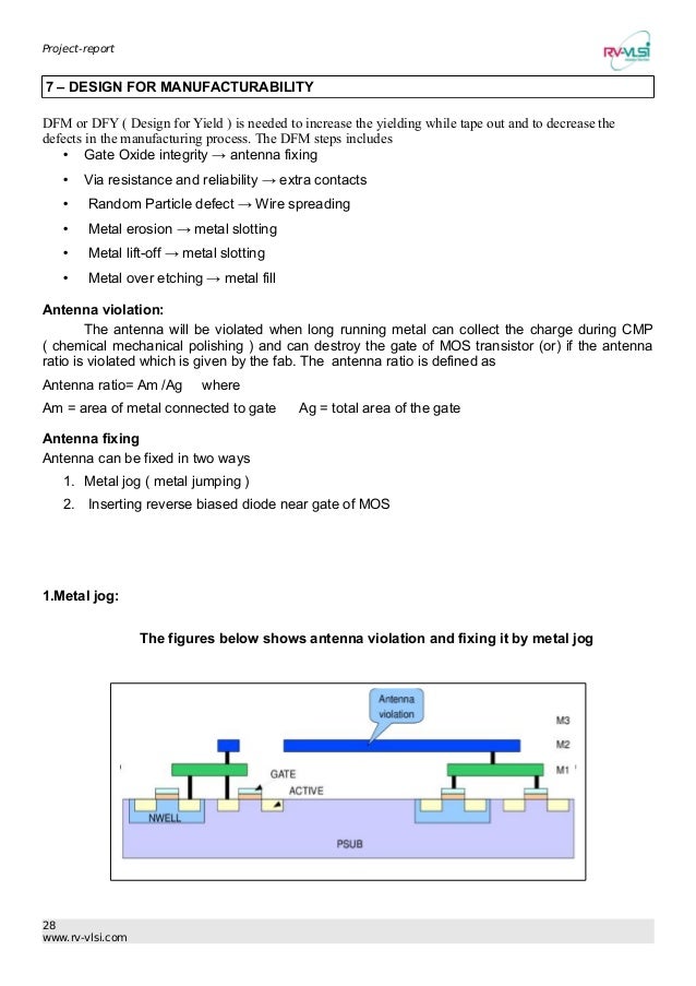
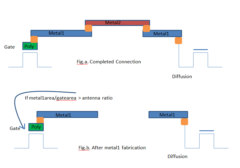
 VLSI Backend Design: Antenna Effect
 Vlsi
Vlsi
 VLSI Backend Design: Antenna Effect
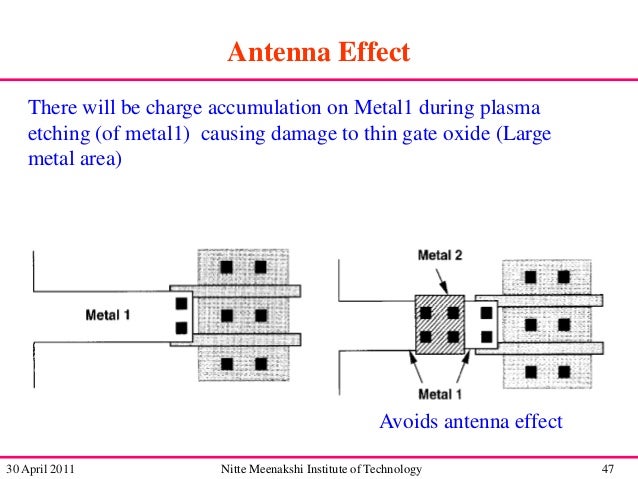
 Antenna Effects |VLSI Concepts

 Antenna Effects |VLSI Concepts
 Smart Antenna - PowerPoint Slides
 Antenna Effects |VLSI Concepts
 Antenna violations resolved using new method - EDN
 Full-Custom Design …. TYWu. Outline Introduction Transistor Process Steps Layout Schematic R/C Design Rules Tools. - ppt download
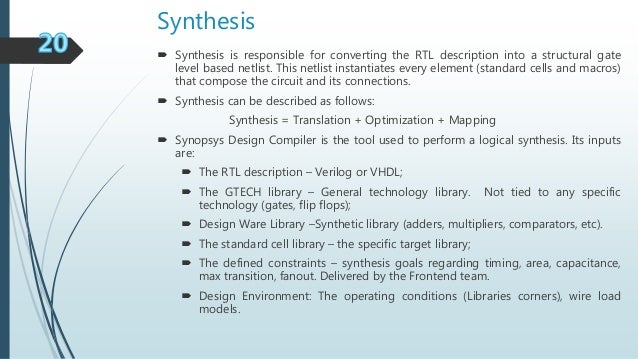
 ppt - UCSD VLSI CAD Laboratory
 pramod
 PPT - Noise and Power Tradeoffs in CMOS Front Ends PowerPoint Presentation - ID:5253285

 Analog Layout design
 VLSI Backend Design: Antenna Effect
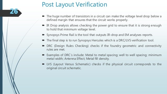
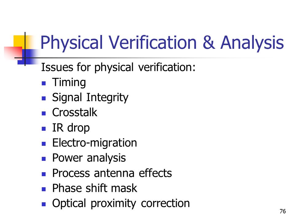 Design Verification for SoC 晶片系統之設計驗證 - ppt download
 Vlsi
Vlsi
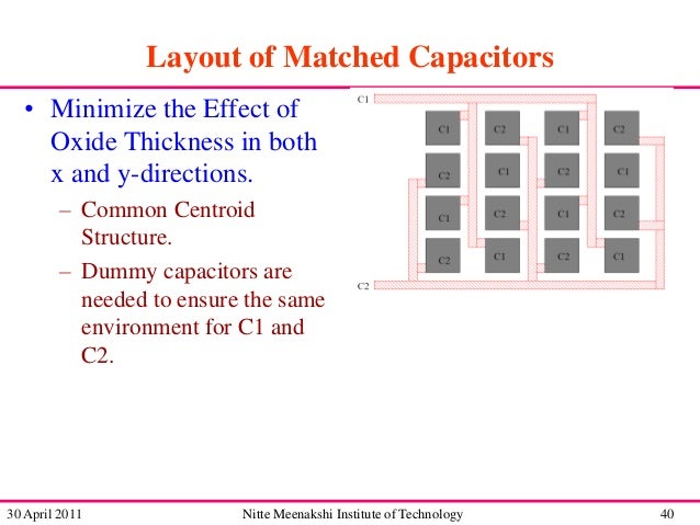 Analog Layout design
Antenna Effects |VLSI Concepts
 Smart Antenna - PowerPoint Slides


Komentar
Posting Komentar